
Cq40 is commonly using and very often find a laptop and its circuit is very basic similarities with other hp models. So I explained it’s main power source B+ Supply section with hp adaptor introduction First. it is Operate with hp’s 3 pin adapter architecture. It is very often used by other companies like Dell, Lenovo, etc. It protects the system with external overvoltage and surges. When there is damage to the circuit it stops output from the adaptor. ID signal is used to operate the charging Enable function.
There are two operations made when plugging in an adaptor:
1. Enable B+ supply through an adaptor
2. Disable supply through a battery
Enable B+ supply through hp adaptor Introduction
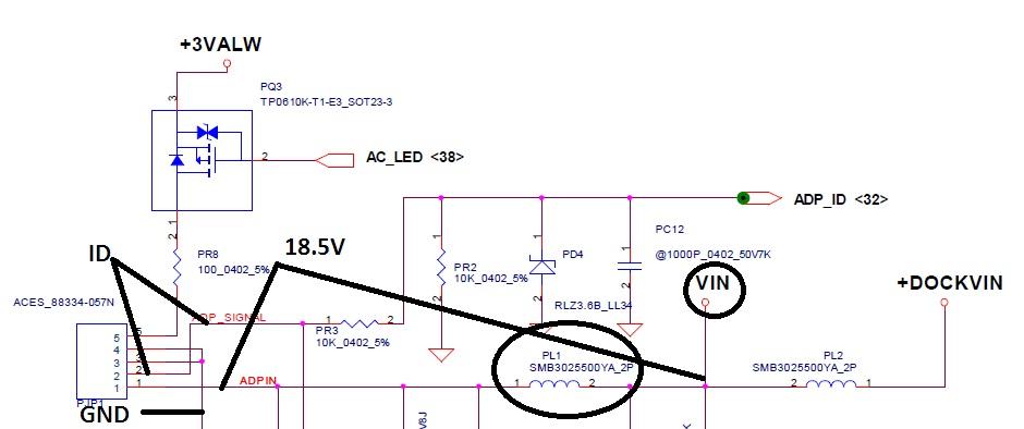
So when Adaptor is plugged in voltage (dc jack pin no.1 adpin) through PL1 signal VIN
it is usually 18.5V. Vin is going through Drain to Source PQ101 to p2 signal before generating p4, GateB+, and CHG_B+ necessary to drive down gate voltage of PQ103 for Source to drain unlock.
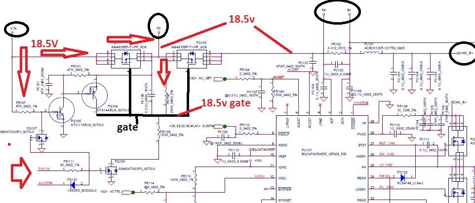
HighThe gate voltage of pq103 is control by PQ109 with PACIN Signal. When PACIN signal high it drives PQ109 gate and Drain to the source of PQ109 open and drop gate voltage of PQ103 through PR109(150k) resistance. voltage B+ generated through PQ103, this is the main system Voltage which is required for high side MOSFETs of supply sections.
Disable supply through battery:
When Adaptor is present VIN through PR103 is present at the gate and makes PQ102 gate high for reverse protection it block a high voltage of the adaptor which is usually 18.5v to attack battery batt pin of the battery connector. ACOFF# high through pd101 ACOFF# make pq102 gate high enable when the adaptor is present.
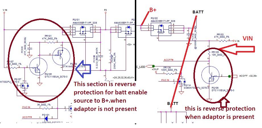
When the adaptor is not the present Acoff signal is come and PQ105 low ACOFF# low and battery supply enables B+ high With appropriate amp.
Under-voltage and Overvoltage Detection:
Cq40 has an external section for under and over voltage section in the latest charging ic has inbuilt this section and operate directly by an acdrv signal. But in CQ40 done by lm393 comparator ic. PU102 (LM393) 8th pin power p2 power from a source of pq102 and pq103 through pr125(47omh). Pin no.6 has fixed voltage 1.24Vref which is maintained by PU104 ic through PR136. PIN no 5 is get voltage from voltage divider bridge made by PR126 and PR133.if pin 5 has a voltage higher than pin6(1.24v) pu102 output to pin7 (pacin) makes high. If a voltage is lower than pin6(1.24v) no voltage on pin7(PACIN).It is under-voltage protection.
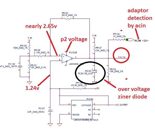
When Pin5 has voltage is higher than 3.15 or zanier diode PD103 capacity PD103 short to ground to protect
Overvoltage.
LED indicator Enable:
PACIN drive also pq114 MOSFET which low gate voltage of PQ3 which open source to drain supply
And led compete it circuit and begin to glow.
By this tutorial, we can only get B+ voltage or main Voltage for System for CQ40 which is necessary to operate
Laptop later we see on charging operation.