
A laptop battery is charged by an external power. Which is usually output dc voltage and provides power to system and charge battery simultaneously. When battery fully charged continue supply to the system through the adaptor and cut battery charging. Every laptop has its type of configured battery charging circuit. The charging process is managed by multi-controllers like:
• Charging ic
• KBC I/O controller (for battery temperature, level, enable and adaptor detection)
• Battery internal ROM chip or external ROM u28 (battery must be connected)
First of all system supply B+(main supply source) is available for system startup
Note: for more on B+ Supply Read Article

ADP_ID or Adaptor Id pin Function: (fault cause: unknown adaptor or not battery charging)
When an adaptor is connected output trough adaptor ID pin (center pin of the adapter) output voltage about 14.V to 18V after this PR3 and PR2 voltage divider drop voltage to 3.3v and it goes to KB926
I/o controller pin no.66 in AD input section. It converts this analog signal to digital which is necessary to identify adaptor type (60w or 90w). If ADP_ID signal is no voltage or below 2V
It shows an unknown adaptor type or not charging due to wrong id detection in windows.
Note: CLK for enabling charging another signal is important like batt temp,batid, batdata a CLK lines
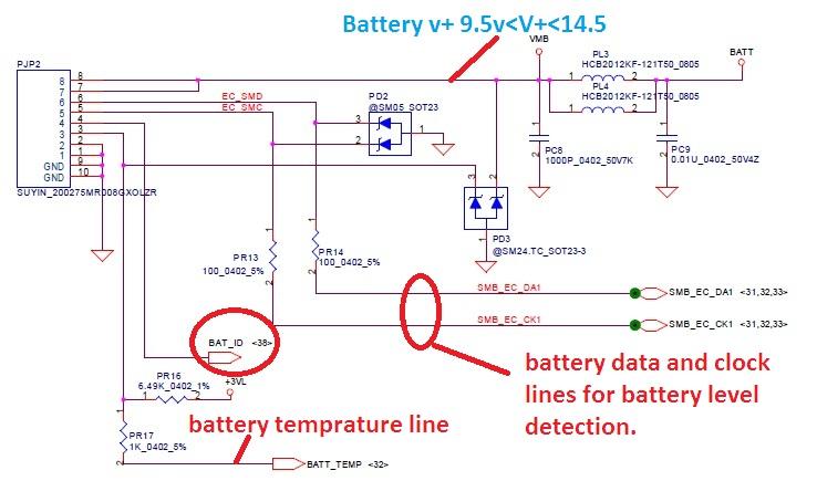 Battery identification and Level detection (fault cause: no battery detect)
CQ40 Battery connector has 8pins:
1. ground
2. ground
3. Battery temperature batt_temp signal (when the battery is connected it is below 2.7v (batt_temp) or about 1.4v.when it is 3.3v no battery is present. It goes to I/O pin no. 63 AD input section)
4. Battery ID bat_id signal (this signal is for battery identification to describe battery type and several cells used in battery .it goes to charging ic pin no.20 (cells).
5. Battery SMBus clock signal ( this signal is for the clock to run data between I/O pin no 77 and battery.)
6. Battery SMBus data signal ( it transfer data between I/O pin no.78 and battery for determining how much battery is charged. It is responsible for making fstchg signal high to enable charging if the battery is low from its full condition.
7. Battery V+ voltage for system supply( It go through pq102 to B+ main supply source)
8. Battery V+ same as pin no 7.
Batt_temp pin no.3 is for battery identification that battery is connected and in good temperature.it is below 3.3 v for detect battery. If it is 3.3v no battery detected.
For battery level ec_smd and ec_smc signals are responsible it should be at 3.3V always.
Adaptor detection for charging IC and Enable charging:
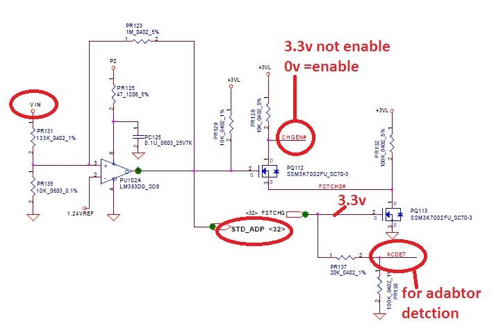
When the adaptor is connected PU102 makes output to pin no.1 when pin no.3 is higher than 1.24vref. when pu102 pin no.2 is high it goes to I/O chip for ac adaptor connect information
To system with the requirement and on PQ112 gate pin no.2 for convert fstchg# to chgen# for enabling or disable charging. As given above
1. adapter is connected adp_id is senses
2. battery is connected batt_temp lower than 3.3v
3. SMBus is connected and has 3.3v and the battery is not fully charged
I/O chip release FSTCHG signal to pq113 which goes to ACDET pin no5 to PU101(charging ic)
When acdet is above 2.4v charging ic detect a valid adaptor for charging.PQ113 gate gets fstchg signal it switches down to low chgen# signal for enabling charging.
There are other pins also which should make some requirement for proper charging
• PVCC pin no.28 is higher than 5v (must be high for all bias enabling)
• Acdet pin no.6 is higher than 2.4V(under-voltage is enabled when lower than 2.4v) and lower than 3.15(overvoltage is enabled when higher than 3.15v)
• Chgen# pin no.1 is low to 0v(0v=enable, 3.3v=disable)
It makes output on vref pin no10 (3.3v) which is connected to cells pin no.20 for 4cell battery
Charging condition available. There is another output on region pin no.24(6v) for boost battery charging.
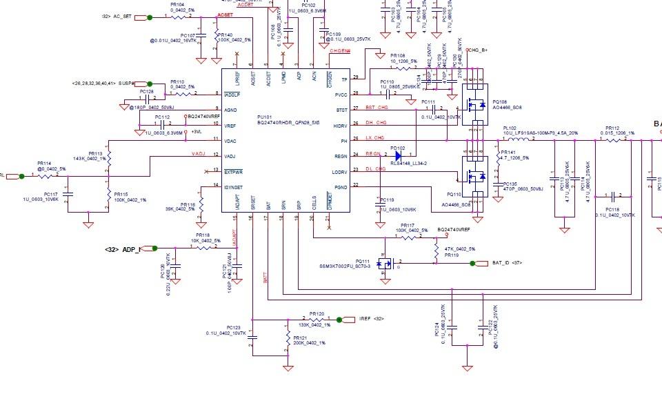
Adaptor current sensing and input:
For adaptor current sensing Charging ic gets input to internal comparator from pr102 at ACP pin no.3 and ACP pin no.2 which compare difference and output ADP_i pin no.15, it goes to I/O pin no.65 AD input. I/O output ACSET from pin no.72 for set adaptor current set pin no.6 of charging ic.
VDAC pin no11 is connected to 3.3v always for reference input for vadj pin no 12 by voltage divider set charge voltage. It is from 2.4 to 3.6 v idle.
Charge current is set by SRSET pin no.16 by the external voltage from I/O Iref signal.
When given condition meets the battery charging process started:
• CHGEN is LOW;
• Adapter is detected;
• Adapter is higher than PVCC-BAT threshold;
• Adapter is not over-voltage;
• REGN(6V) and VREF(3.3v) are valid;
• Thermal Shut (TSHUT) is not valid(temperature should be under 130 degree)
Charging is enabled (chgen# =0v) charging ic makes output on the gate of high side MOSFET PQ108 and on the gate of low side MOSFET PQ110 for charging voltage produce on pin no 25 (ph) through pl102 to the battery.
Battery Full Charge detection:
Voltage through pr112 to battery and charge battery, charge current and voltage difference id detects by SRP pin no.19 and SRN pin no.18 .when SRP and SRN have true(SRP>SRN) IC regulate the charge MOSFET gate. When SRP=SRN it stops output on hdrv and ldrv to stop battery charging. it is battery over-voltage condition when the battery is charged up to 104% (detect by BAT pin no.17) it stops charging .it never starts again until battery falls to 102%.