
CQ40 laptop Standby supply
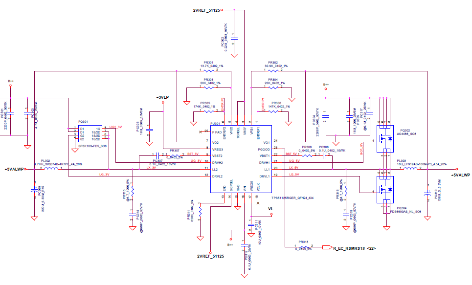
If CQ40 laptop has a good B+ main supply which necessary for the system to turn on always supplies(3VL and 5VL). Always supply is to maintain the system in a ready state before pressing the power button.TPS51125 is used in CQ40 for laptop standby supply regulation.
Note: Check B+ and Charging supply Articles for Details
LDO or Standby section
In Compaq CQ40 B+(18.5v) supply apply to pin16 of tps51125 It receives power supply for ic’s LDO (3.3v and 5v) laptop standby supply section and makes EN0 pin13 high and connect to GND with 620k resistance. EN0 is the control pin of VREG5 pin17, VREG3 pin8, and VREF pin2 regulators.
Bring this node down to GND disables those three regulators and minimises the shutdown supply current to 10 μA. Pulling this node up to 3.3 V or 5 V will turn the three regulators on to standby mode.
Given below table is shown the sequence:
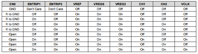
VREF volt which is typically 2v fix voltage which is connected to TONSEL pin4 for set ch1 and ch2 frequency to 245KHz and 305KHz respectively and VREF is also connected with SKIPSEL for auto skip function. It also supplies inner logic for VREG5 and VREG3 laptop STANDBY SUPPLY.
VREG5 and VREG3 STANDBY SUPPLY output respectively with 100mA load The VREG5 serves as the main power supply for the analog circuitry of the device and provides the current for gate drivers.
The VREG3 is intended mainly for auxiliary 3.3-V supply for the notebook system during standby mode. It provides supply to I/O chip, on-off logic etc.
Note: in CQ40 VREG5 is +5VL and VREG3 is +3VL
Turn ON switch mode power supplies (channel-1, channel-2)
When LDO section enables the two switch mode power supplies (channel-1, channel-2) become ready to enable at this standby mode.
The TPS51125 has an internal, 1.6 ms, voltage servo soft start for each channel.
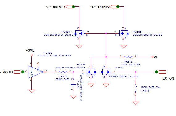
Each Channel is enabled by ENTRIP1 pin1 and ENTRIP2 pin6 respectively.
For this, there is a little logic.There are types of input to make high both ENTRIPx one is ACOFF and second is EC_ON. ACOFF is input when an adaptor is inserted in DC JACK I/O makes low ACOFF signal by NOT GATE (74lvc14 ic)logic output
On the gate of pq308 and drop down Drain Voltage to GND by this Gate voltage of both pq305 and pq306 is low and high the Drain voltage which is EnTRIP1 and ENTRIP2.
When the ENTRIPx pin becomes higher than the enable threshold voltage, which is typically 430 mV, an internal DAC begins ramping up the reference voltage to the PWM comparator and make the gate voltage high and both channels are enabled output +3VALWP and +5VALWP STANDBY SUPPLY respectively.
When all output is good it releases power good signal from pin23 for Ec to release RSMRST#.
Over Voltage And Under Voltage Protection
TPS51125 monitors a resistor divided feedback voltage to detect over and under voltage .which is usually
Done by VFB1 pin2 and VFB2 pin5.
When the feedback voltage becomes higher than 115% of the target voltage, the OVP comparator output goes high and the circuit latches as the top MOSFET driver OFF and the bottom MOSFET driver ON.
TPS51125 monitors VO1 pin24 and VO2 pin7 voltage directly and if it becomes greater than 5.75 V the TPS51125 turns off the top MOSFET driver.
When the feedback voltage becomes lower than 60% of the target voltage, the UVP comparator output goes high and an internal UVP delay counter begins counting.
After 32 μs, TPS51125 latches OFF both top and bottom MOSFETs drivers and shut off both drivers of another channel. This function is enabled after 2 ms following ENTRIPx has become high.